Sputtering generally means to eject atoms from a solid-state target by “bombarding” it with accelerated gas ions. This technique is often used for the deposition of thin films. Therefore a gas discharge is ignited in an inert gas (i.e. argon). The positive gas ions are accelerated towards a negative charged target where they eject atoms by direct momentum transfer. These atoms diffuse into the vacuum chamber and then condense as a thin film on the substrate. Furthermore secondary electrons, which keep the gas discharge in constant renewal, are set free. The most used sputtering techniques are reviewed below in a very general fashion:
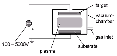
Fig. 1 shows the arrangement used for DC-sputtering. Here a target and substrate oppose each other in the vacuum chamber having a distance of a few centimeters. The target is connected to the negative output of a DC power supply, acting as the cathode and the substrate and chamber walls act as the anode. After the creation of an argon atmosphere with a pressure of about 10-3 to 10-2 mbar, the gas discharge is then ignited, by applying a DC voltage. The created Ar+-ions are then accelerated towards the target and eject atoms from which the thin film is deposited on the substrate.
Fig. 1
DC sputtering works with all conductive target materials. It is impossible to sputter insulating materials with this technique because the positive charged ions can’t flow through the insulator. The electric circuit is interrupted. So the potential at the cathode drops and the positive ions are no longer accelerated towards the target and the process ends.
RF-SPUTTERING
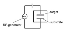
To sputter insulators as well as conducting materials another technique is used, RF-sputtering (see Fig.2). In the RF-circuit a negative DC-potential builds at the target (self-bias). This phenomenon is caused by the different mobility of heavy ions and light electrons in a high-frequency electric field. After the creation of an argon atmosphere in the vacuum chamber, the Ar+-ions are accelerated towards the target and eject atoms from it. Because the positive charges don’t need to flow through the target the sputtering of non-conducting materials is also possible. Furthermore the plasma has a higher level of ionization caused by the oscillating movement of the electrons in a radio-frequency field. Therefore the current conduction is higher and lower voltages can be used at same power levels. This has an important advantage: less damages to the deposited film than with the DC-process above. Here is more information on RF Sputtering.
REACTIVE SPUTTERING
Another variation of sputtering is the reactive process, which also can be performed with the DC- as well as, the RF-techniques above. In the conventional process the target is made of the same material as the deposited film and the gas used is normally pure argon. The thin films, which are made with the reactive process, are a chemical compound of the target material and the reactive gas. This gas (i.e. oxygen or nitrogen) is mixed with the argon during the process. The atoms or molecules of both substances react in the plasma and the thin film is formed of the reaction product. So, TiN- or ITO-films can be deposited as an example. Along with sputtering there are other coating processes using plasma such as PECVD (plasma enhanced chemical vapor deposition) or ion plating.


